
Reduce time to wafer scaling with the new HORIBA LabRAM Odyssey Semiconductor microscope
👉 “How uniform is the layer over the entire wafer?”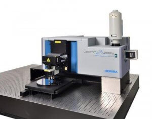
👉 “How can we automate uniformity assessment for a series of wafers?”
👉 “What is the nature of the defects?”
Wonder no more! There is now a microscope that can accelerate your process optimization by achieving Raman/PL mapping of wafers up to 12” in diameter in a fast and reliable way.
The DuoScan™ imaging technology offers two confocal imaging modes: The macro-mapping mode for fast full wafer mapping, and the step-by-step mapping mode to investigate detected defects.
Automating your full Raman/PL characterization routine is made easy by creating and using a “method”, a recipe containing all acquisition, data processing, display, and analysis operations, all accessible with one click in the LabSpec6 software.
The HORIBA LabRAM Odyssey Semiconductor qualifies any semiconductor material, thereby addressing a large panel of applications including microelectronics, data storage, LED, photovoltaic and other related nanoelectronics industry R&D.
Contact us to know more about HORIBA instruments for semiconductor reasearch and applications!